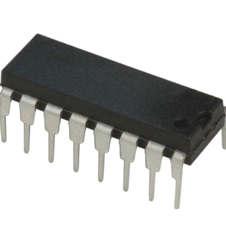
CD4511 BCD to 7 segment latch/decoder/driver
KSh 150.00
Features of CD4511
- Has a lamping test and blanking capability.
- Has Low logic circuit power dissipation.
- An Input latches for BCD code storage.
- Also has a Balanced propagation delays and transition time.
- High output sourcing capability.
- Moreover, has a Lamp intensity modulation capability.
- Lastly, has a Rigid structure.
Technical Specification
- Its supply voltage ranges from 3v to 18v
- Time setup is 150, 70, and 40ns at 5v, 10v, and 15v respectively
- Strobe pulse width is 400, 160, and 100ns at 5v, 10v, and 15v respectively
- Hold time is zero
- 100% tested for quiescent current at 20v
- Having high input current of 1uA (max.) at 18v
- Maximum output current sourcing of 25mA
- Additionally its operating temperature ranges from -40 °C to 85 °C
- Lastly, its Storage temperature ranges from -65 °C to 150 °C
Description
CD4511 is a BCD to 7 segment latch/decoder/driver with four address inputs (A, B, C, D). It has a latch enable input (LE) and a ripple blanking input (BI). It also has a lamp test input (LT) and seven segment outputs (a to g). When LE is LOW, the state of the segment outputs (a to g) is determined by the data on A to D. As LE goes HIGH, the last data present on A to D are stored in the latches and the segment outputs remain stable. When LT is LOW, all the segment outputs are HIGH independent of all other input conditions. With LT HIGH, a LOW on BI forces all segment outputs LOW. The inputs LT and BI do not affect the latch circuit. Inputs include clamp diodes. Thus enables the use of
current limiting resistors to interface inputs to voltages in excess of VCC
Features of CD4511
- Has a lamping test and blanking capability.
- Has Low logic circuit power dissipation.
- An Input latches for BCD code storage.
- Also has a Balanced propagation delays and transition time.
- High output sourcing capability.
- Moreover, has a Lamp intensity modulation capability.
- Lastly, has a Rigid structure.
Technical Specification
- Its supply voltage ranges from 3v to 18v
- Time setup is 150, 70, and 40ns at 5v, 10v, and 15v respectively
- Strobe pulse width is 400, 160, and 100ns at 5v, 10v, and 15v respectively
- Hold time is zero
- 100% tested for quiescent current at 20v
- Having high input current of 1uA (max.) at 18v
- Maximum output current sourcing of 25mA
- Additionally its operating temperature ranges from -40 °C to 85 °C
- Lastly, its Storage temperature ranges from -65 °C to 150 °C
CD4511 Equivalent ICs
74LS47, SN5446A , SN5448, SN54LS48, 74LS48, SN74LS49, SN7448
/ / / / / / /


Reviews
There are no reviews yet.