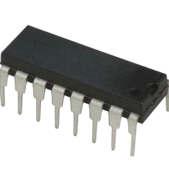
CD4053 Triple 2-Channel Analog Multiplexer/Demultiplexer
KSh 100.00
Features of CD4053
- Fully static operation
- 5 V, 10 V, and 15 V parametric ratings
- Standardized symmetrical output characteristics
- Specified from -40°C to +125 °C
- Complies with JEDEC standard JESD 13-B3.
- Wide range of digital and analog signal levels: digital 3 to 15V, analog to 15Vp-p
- Low “ON” resistance: 80Ω (typ.) over entire 15Vp-psignal-input range for VDD − VEE = 15V
- High “OFF” resistance: channel leakage of ±10 pA (typ.) at VDD − VEE = 10V
- Logic level conversion for digital addressing signals of 3 – 15V (VDD − VSS = 3 – 15V) to switch analog signals to 15 Vp-p (VDD − VEE = 15V)
- Matched switch characteristics: ∆RON = 5Ω (typ.) for VDD − VEE = 15V
- Very low quiescent power dissipation under all digital control input and supply conditions: 1 µ W (typ.) at VDD − VSS = VDD − VEE = 10V
- Binary address decoding on chip
20 in stock
Description
CD4053 is a triple 2 Channel multiplexer with three separate digital control inputs. That is; A, B, and C, and an inhibit input. Each control input selects one of a pair of channels which are connected in a single pole, double throw configuration. It is a digitally controlled analog switch having low ON impedance and very low OFF leakage current.
Features of CD4053
- Fully static operation
- 5 V, 10 V, and 15 V parametric ratings
- Standardized symmetrical output characteristics
- Specified from -40°C to +125 °C
- Complies with JEDEC standard JESD 13-B3.
- Wide range of digital and analog signal levels: digital 3 to 15V, analog to 15Vp-p
- Low “ON” resistance: 80Ω (typ.) over entire 15Vp-psignal-input range for VDD − VEE = 15V
- High “OFF” resistance: channel leakage of ±10 pA (typ.) at VDD − VEE = 10V
- Logic level conversion for digital addressing signals of 3 – 15V (VDD − VSS = 3 – 15V) to switch analog signals to 15 Vp-p (VDD − VEE = 15V)
- Matched switch characteristics: ∆RON = 5Ω (typ.) for VDD − VEE = 15V
- Very low quiescent power dissipation under all digital control input and supply conditions: 1 µ W (typ.) at VDD − VSS = VDD − VEE = 10V
- Binary address decoding on chip
Applications
- Analog multiplexing and demultiplexing
- Digital multiplexing and demultiplexing
- Signal gating
Equivalents
CD4051, CD4052


Reviews
There are no reviews yet.